Open your PCB in your favorite CAD tool and change the grid system of your CAD to 50 mil. You can change this back to whatever else you want, once you complete the placement of the RapidStencil components as described in this section


Depending on the size of your board and the size of your RapidStencil, you need to add the appropriate guide device component to the schematic (either GUIDE_10x10 or GUIDE_20x20). Bring 4 components labeled as PIN_LARGE_SINGLE_DEVICE and another 4 components named PIN_SMALL_SINGLE_DEVICE into your schematic design (pic #1).
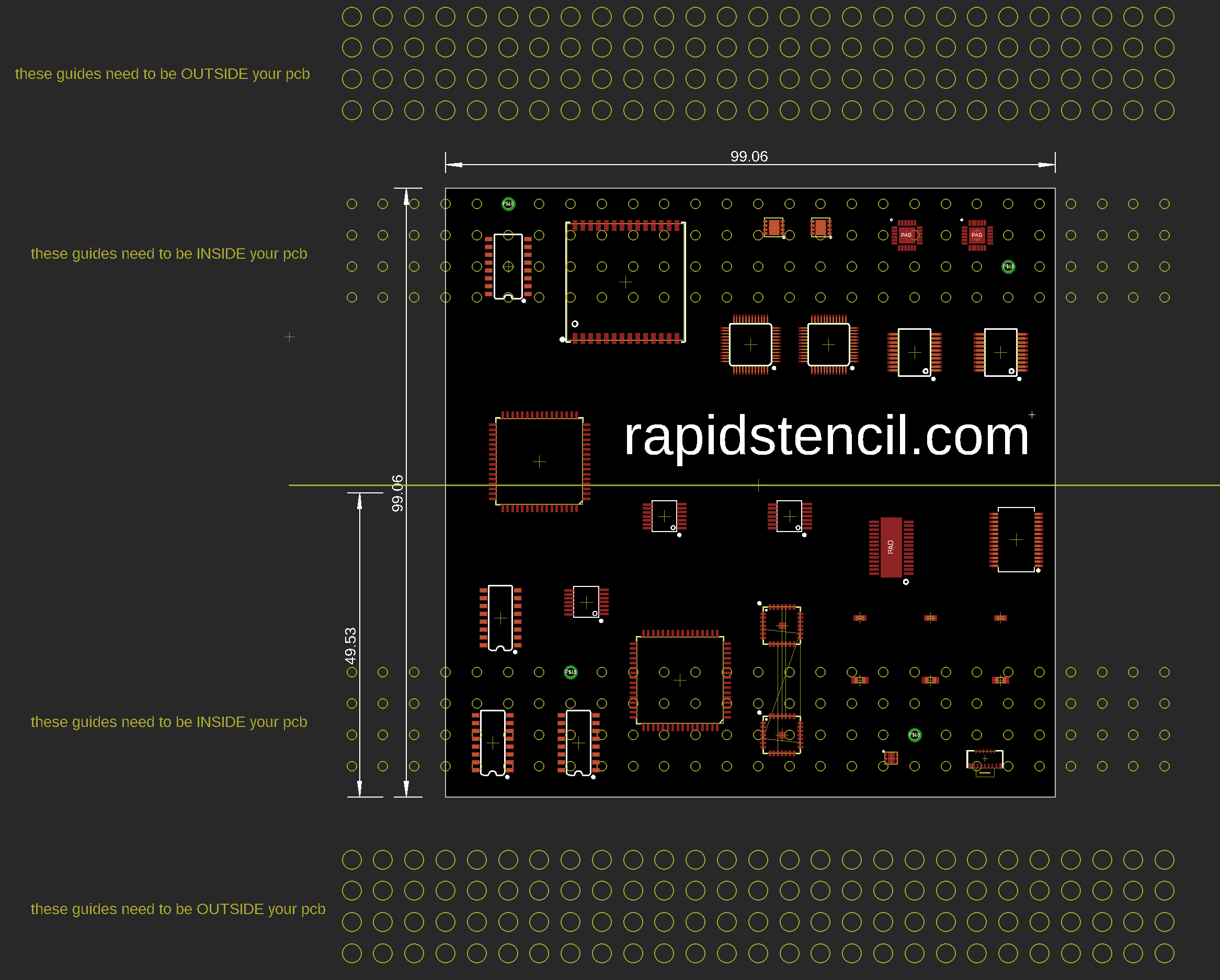
The guide component (GUIDE_10x10 or GUIDE_20x20) depending on the size of your board) has a diagram on the documentation tDocu layer to assist you with positioning it correctly. If it doesn’t appear on your PCB board you need to enable the layer on your CAD software. Look at our FAQ to see how you can do that in EAGLE. You need to move it around your PCB so its middle line is close (but it doesnt have to be exact, if it is though you can save yourself a few minutes the first time you use Rapidstencil with your new PCB board; See Nice to have) to your PCB middle line.
Nice to have. If you manage to put the diagram right at the center of your PCB, then you can use the diagram as it is positioned, to take note of the pin coordinates on the RapidStencil. You will need them when your are placing the pins on RapidStencil, when you will apply the solder paste on your boards. If you didn't, then it's not a big deal. You can either calculate them by determining the shift of the diagram relative from the center or you will locate them using the stencil on the RapidStencil during the first time when you will apply solder paste on your boards. We explain how later in this guide.
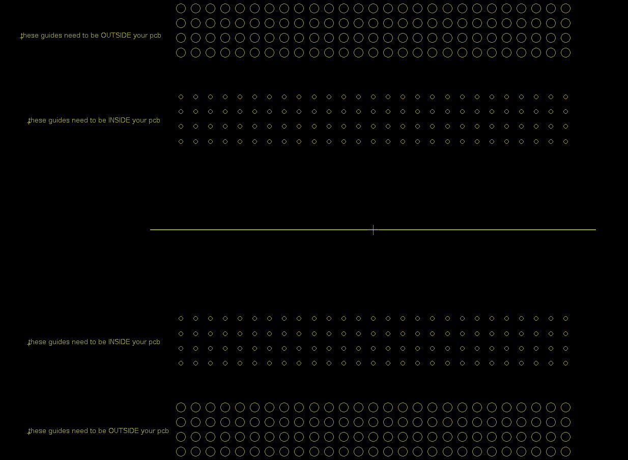
Prerequisite 1. At least a portion of both top and bottom inner bands (the ones with the smaller holes with labeled a,b,c,d and w,x,y,z) need to be located inside your PCB. There are indicators on the guide that clearly identify which holes need to be inside your PCB area “these guides need to be INSIDE your pcb”. These will be used to align your PCB’s on the RapidStencil using the small pins. Not all smaller holes need to be inside your PCB. It’s enough if only the last or the first row from either are inside your PCB (rows d and w).
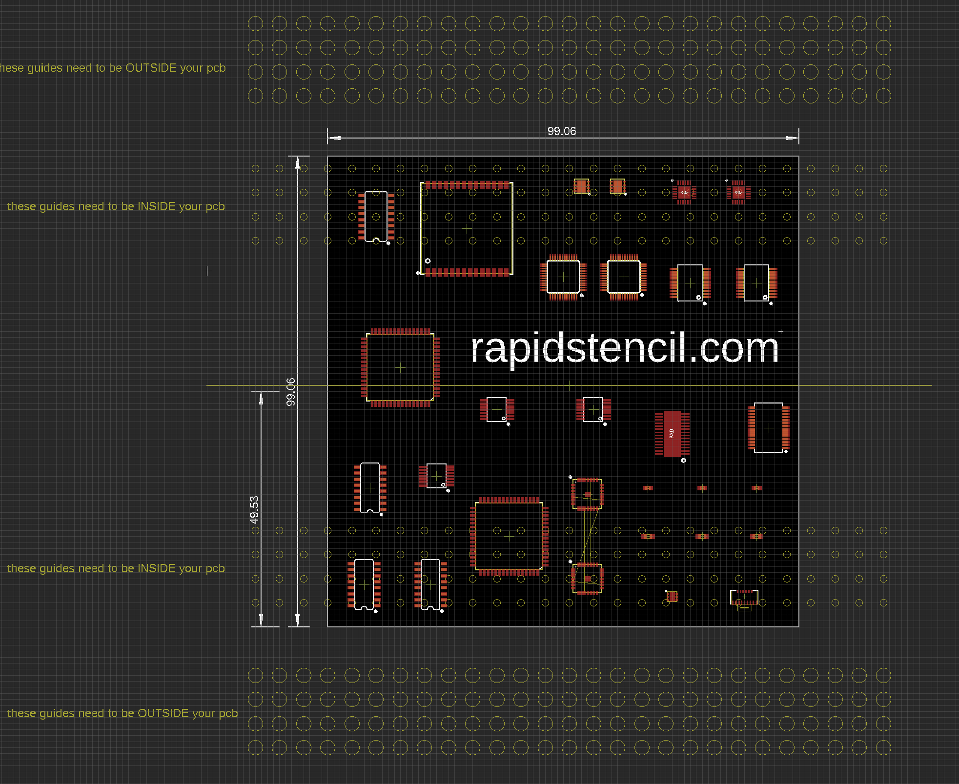
Prerequisite 2. At least a portion of the top and bottom rows (rows A and Z) with the larger holes need to be located outside of your PCB area.This will happen automatically if you are using the right RapidStencil size for your PCB. If it doesn’t happen (all of the rows of larger holes of one band are located within your PCB) then you need a larger RapidStencil size. Your PCB is too big and you need to get the next size larger RapidStencil (try the guide_20X20 rather than the guide _10X10 to be sure). If the 20x20 doesn't fit your boards, please contact us in case we can custom make it. These larger holes, will be used to align the stencil with your PCB and RapidStencil. This is how it looks on the PCB (pic 3) after your position it correctly
If the first or the last row of the top and bottom outer bands (row A and Z), with the larger holes, are located inside your PCD then the positioning of the guide components is NOT valid and you either need to reposition the component or get the next size of RapidStencil.
Position the SMALL pins: Place the 4 small pins (PIN_SMALL_SINGLE_DEVICE) EXACTLY on top of small pin section of the diagram (snap them to grid). Since your grid is 50 mil you should have no problem doing this. They need to coincide exactly with the pins on the diagram so they will be aligned with the RapidStencil pin placement. If they don't, change your grid size to 50 mil and snap the diagram to the grid close to the center of the PCB again. if the grid is set to 50 mil then it's guaranteed to coincide by design (pic 4)
Ensure that all 4 small pins are located INSIDE of your PCB. You need at minimum 3 small pins inside of your PCB to keep your board tight on RapidStencil
Position the LARGE pins: Place the 4 large pins (PIN_LARGE_SINGLE_DEVICE) EXACTLY on top of large pin section of the diagram (snap them to grid). Since your grid is 50 mil you should have no problem doing this. They need to coincide exactly with the pins on the diagram so they will be aligned with the RapidStencil pin placement. If they don't, change your grid size to 50 mil and snap the diagram to the grid close to the center of the PCB again. if the grid is set to 50 mil then it's guaranteed to coincide by design
Ensure that all 4 large pins are located OUTSIDE of your PCB. You need at minimum 3 large pins outside of your PCB to keep your stencil tight on RapidStencil
Please note the coordinates of the pins. You will need them when you will assemble RapidStencil and apply solder paste on your boards. If you don't then you might need an additional step to find out what they are.
Click on the picture to view in detail
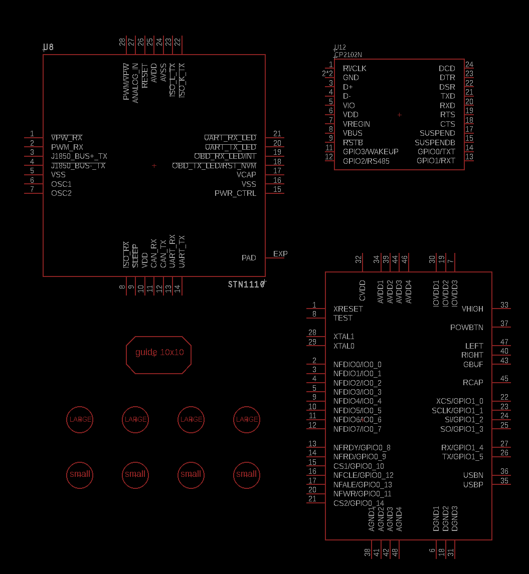
RapidStencil components into the schematic, 1 10x10 guide, 4 small pins, 4 large pins
RapidStencil guide. Place it close to the middle/center of your PCB,
Center line of guide is close to the center of the board, some of the smaller holes are inside your board area and some of the larger holes are outside your PCB
Place the 4 SMALL pins EXACTLY on top of small pin section of the guide INSIDE of your board
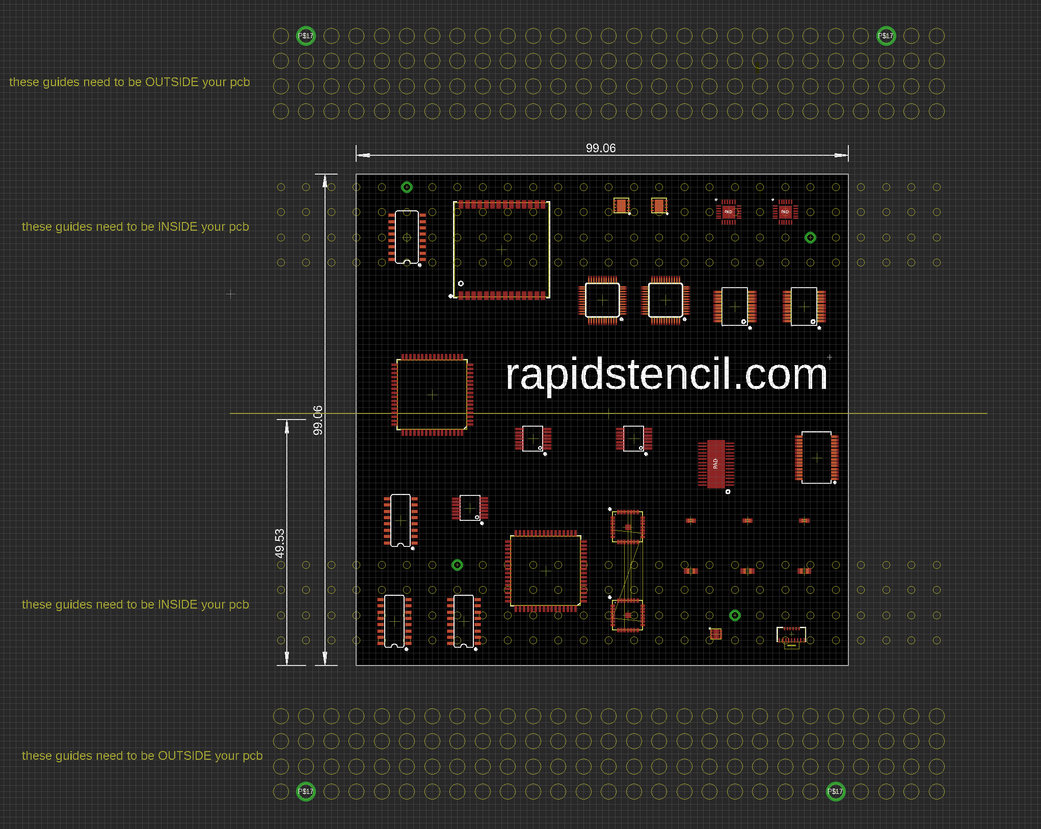
Place the 4 LARGE pins EXACTLY on top of large pin section of the guide OUTSIDE of your board